
Introduction
The cadence tools we are using are: IC 5.0 and LDV 5.1. We have also installed the NCSU_CDK 1.5.1 on top of that. Because of this, menus are generally customized and we can use MOSIS design processes for layout design. The tools we are going to use include:
- Virtuoso layout editor
- Virtuoso schematic composer
- Affirma Verilog simulator
- Assura physical verification tools
- Spectre device simulator
Setting up the environment
There are two things we need to set up, the X-windows display settings and the Cadence tool environment settings.
- X-windows display settings
The cadence tools are now installed on Linux machines in ITEB C27. The Linux machines names are "cselin6.engr.uconn.edu" (cselin2-cselin10). Assume you use Unix or Linux on a local machine, you have to use the following command to login cselin6 and enable remote display.
-
ssh -X username@cselin6.engr.uconn.edu
If you use windows instead, you have to get X-win pro, Exeed, or Cygwin in order to display the X-windows stuff.
When you start Exceed, you will see a task "exceed" on the task bar, right click on it, and a menu will pop up. Go to "tools->toolbar" and toggle on "show". Now a toolbar window shows up.
Click on the first icon on the bar "client setup" and click on "new ...". A window "Xstart Client startup Application" pops up. Fill in your user name and password. Type "cselin6.engr.uconn.edu" in host and use "Linux" for host type. Use xterm for the application and then click on "run!" on the menu. Now the x-window starts up.
X-win pro can be set up in a similar way.
For Cygwin, after you start it, type in "startx", a X window will be appearing as the server. - Cadence tool environment setup
Bash is the shell recommended by ECS. Some users might still have csh as the default shell. To change the default shell from csh to bash,remotely log into fester.engr.uconn.edu using ssh, type the command ypchsh, enter the NIS/UNIX password, the path for bash is /bin/bash. For questions about changing the default shell, please contact the ECS Help Desk by phone (486-1821) or by email (help@engr.uconn.edu).
Log into a Linux workstation in ITEB C27, run the script cdsupdate.sh to set up environment/configuration files.
# /apps/ecs-apps/software/ece/cdssetup_6421/cdsupdate.sh
Note that this will cover your own .bashrc and .bash_profile files under your home directory. You have to back up those files before you run the script.
Log off and log in again.
Run icfb to start the program.
# cd ~/cadence
# icfb &
Now we are ready to use Cadence tools.
Starting Cadence
You should always start the Cadence tools from the directory that contains the Cadence user setup information. Assume now you have already created such a directory called "cadence", you can invoke Cadence tools through the following command regardless whichever tool you want to use:
-
icfb &
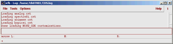
We refer to this window "CIW". CIW displays Cadence log file "CDS.log" stored in your "run" directory. When you use a specific Cadence tool (e.g. Virtuoso) and run a task (e.g. DRC), the result is sometimes displayed in the CIW. So you should check back on this window quite often.
Your Cadence designs (schematic, layout, ...) are organized in the form of libraries. You can go to Tools->library manager to invoke the library manager. Here is a description on how to use library manager.
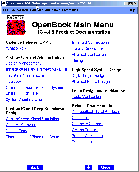
At any time when you run into any problem, you can always read the Cadence document by invoking the "openbook" document through the Help menu. You can also find the documents for all the tools in IC or LDV package by typing
-
openbook /u/cadence/IC445/doc/openbook/menus/menusTOC.obk &
-
openbook /u/cadence/LDV30/doc/openbook/menus/menusTOC.obk &
Library Manager
CIW and Library Managaer window are the two most important windows of
Cadence tools. CIW shows the log information; library manager helps you
manage your designs which are generally organized in a number of cells. Every
time when you start Cadence tools, you would always want to start a library
manager from CIW as well.
When starting a design in Cadence, the first thing to do is to create
a library where you can store your designs. Every Library is associated
with a technology file and it is the technology file that supplies all
the color maps, layer maps, design rules, extraction parameters required
to view, design, simulate and fabricate your design.
- Starting Library Manager
In CIW, click on Tools->Library Manager. The following window appears.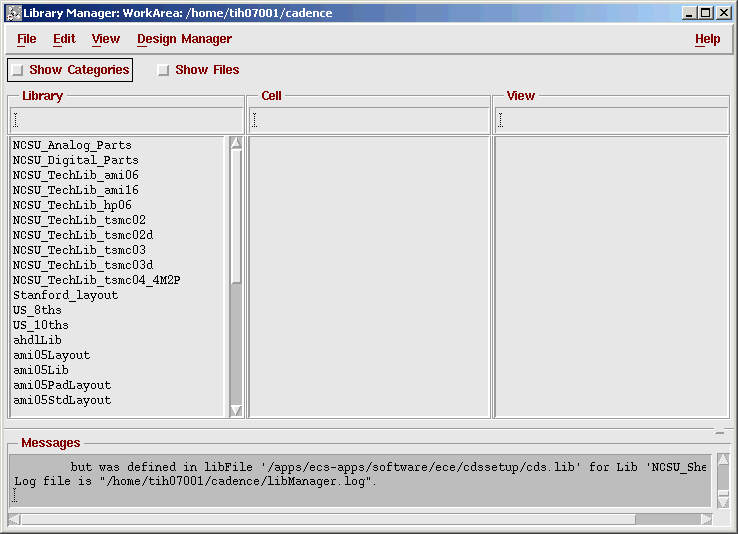
- Create New Library
In Library Manager window, click on File->New ->Library.... You will see the following window. Enter the name of library (example shown: ECE359) where you expect to store your own designed cells. Attach this library to an existing technology (example shown: AMI 0.60 micron technology) so that the Cadence tools would know the technology specifics of your design (like SPICE models, DRC rules, ERC rules, etc.)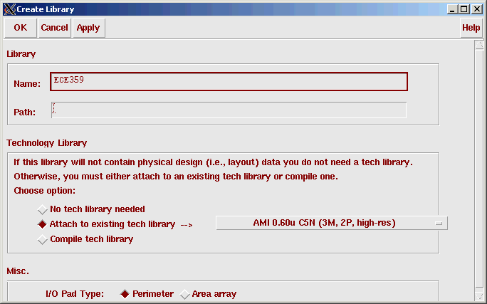
You can also use "compile tech library". This creates a local copy of the technology library in your run directory, thus it is not very efficient in the sense that every use has a copy of an indentical library. It is also not very flexible in the sense if there is any change made to this technology library, each user has to update his copy of the compiled tech library. Because of these two reasons, we prefer "attach to existing tech libary" to "compile tech library".
Now your library manager window should look like follows: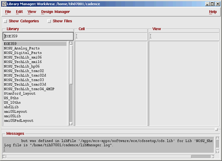
Not only you have created a library "ECE359" of your own, but you have also included its associated technology library "NCSU_TechLib_ami06" in your library path.
- Library Path Editor
Note when we created the new design, we didnot specify the library path in the "Create Library" dialogue box. The default path is under your Cadence run directory. If you want to know the exactly location of all the libraries, you can use "Library Path Editor" to show the library path.
In Library Manager window, click on Edit->Library Path.... The following window appears.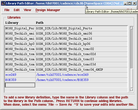
This windows reflects the CDS.lib file in your Cadence run directory. In general, do not attempt to modify the existing library path in the library path editor.
Schematic Composer
At this point, you have created a library (in the example "ECE359") to store your design and can start the design process. For a full custom design, the process begins by creating a schematic. Then we simulate this design to verify the correctness of its functionality and explore its switching behavior in order to optimize the performance. Only after this is done, we will start the layout of the design.
- Create a new schematic
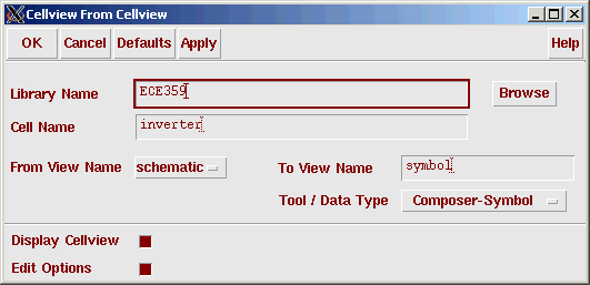
In your Library Manager window, click on the File->New->Cellview. A pop-up dialogue box appears. Click on the library name button and select "ECE359". Click on the Tool button to select "Composer-Schematic". The View Name will automatically change to "schematic". Enter the name of the cell you wish to design in Cell Name. For the tutorial case, we design an inverter.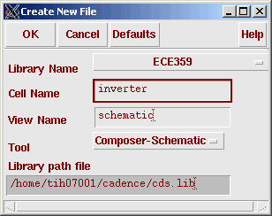
This will pop-up an empty Schematic Creation Window. We will talk about how to create an inverter in this schematic window in the following steps. We will start by adding an instance of NMOS and an instance of PMOS.
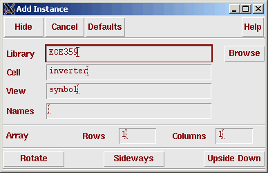
- Add an instance
To place an instance, e.g. an NMOS device, in your schematic, activate the schematic window, then click on Add->Instance (or type i). The "Add instance" dialogue box appears together with the "component Browser" dialogue box. (In case the "Component Browser" does not appear, click on browse in the "Add Instance" dialogue box to start it.)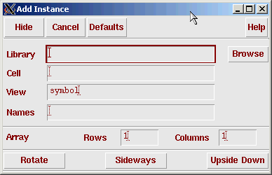
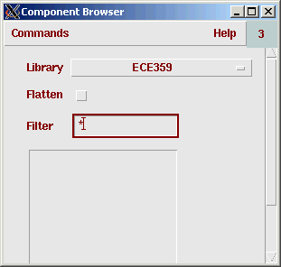
In "Component Browser" window, Click on Library and choose ami05Lib. Click on basic and choose nmos4 as your NMOS device. To place the instance, activate the schematic window and click the left mouse button to put the instance at the place desired.
Note in Cadence schematic composers and layout editors, a command will not terminate unless the user cancels it or the user starts a new command. In this case, you can see another instance is ready to be placed right after you placed the first instance. To terminate the current operation (which is "add instance" in this case), press ESC key on the keyboard. In fact, you can always cancel the current operation in schematic or layout editors by pressing ESC key.
- Set Properties
To set the property of the instance that you just placed or any object in your schematic or layout design, select the object by clicking on it and then go to "Edit->properties->Object..." (or by typing q). An object properties editing form will pop up.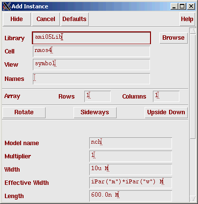
Change the width or length of the gate to the desired value. In this case, we use the default value. Following the same techniques, we can add an instance of PMOS transistor.
- Connect the instances with wires
To connect the PMOS and NMOS devices or any electrically connected devices, click on Add->Wire(narrow) in the schematic window (or type w). Click at the terminal where the wire starts and click at the terminal where the wire ends, a wire will be automatically added. If you are not satisfied with the automatic wiring, you can remove the wire and reroute it manually. This time, instead of clicking at the terminal where the wire ends directly, you can click the left mouse button whenever you want to change the wire direction.
If you want to stop the wire somewhere instead of connecting it to a terminal, double click your left mouse button and a dangling wire is created. In general dangling wire should be avoided, however, in some cases (like you want to label this wire or add a pin to this wire), a dangling wire makes sense.
w
- Create pins and labels
For any cell, we have to specify its input/output behavior. We can achieve this through adding the pins for its input and output. For some global wires (like VDD and GND), we can simplify the I/O of the schematic by adding a label to each one of them.
Click on "Add->Pin..." (or type p) in the schematic window, the following dialogue box would appear.
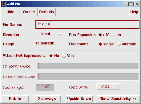
For an input pin, Choose the Direction to be input. Specify the Pin Names (inv_in in the example). Activate the schematic window and click on the left mouse to put the pin. Similarly we can put an output pin (inv_out in the example) to the output of the cell.
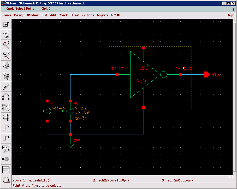
- Check and save the designs
After the design has been completed, click on "Design->Check and Save" to check and save your designs. Check the CIW window to see if there is any errors in your designs. The following image shows the completed design of inverter.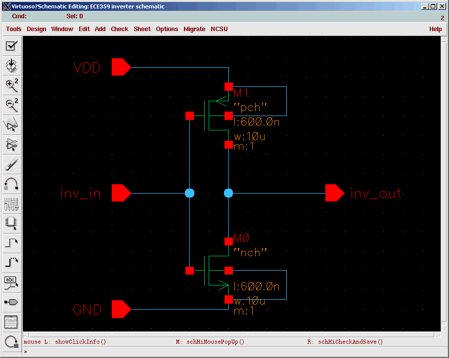
- Hot keys
i: Add instances
q: Edit properties
w: Add wires
p: Add a pin
l: Label a wire
z: Zoom in
Z: Zoom out by 2X
f: fit the schematic in your schematic window
right mouse button: repeat last command
Create Symbols
Symbols are useful when the schematic design is done hierarchically.
At a higher of level of abstraction, we would like to use a symbol to replace
the details of a cell. Because of this, a symbol of a cell design should
define all the inputs and outputs of that cell.
There are two ways to create a symbol. If you have a schematic design
already, you can create its symbol right from the cell. If you don't have
a schematic design yet and you want to create a symbol for the cell, you can
start from scratch.
- Create a symbol from an existing schematic
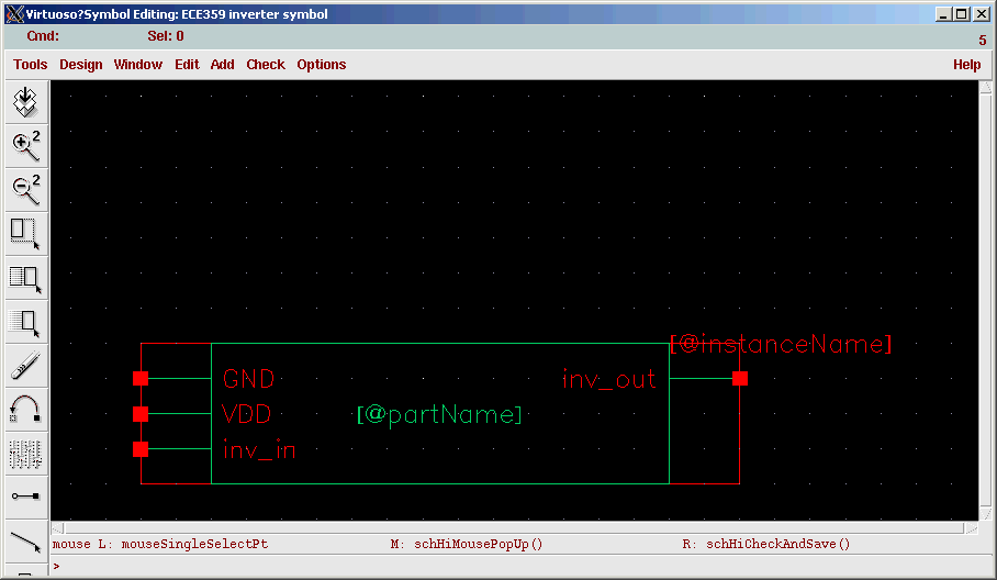
Click on Design->Create Cellview->From Cellview menu in the symbol edit window, a pop up dialogue box will appear. We can use the default setup in this window to create the symbol.
This will pop-up another window that contains a default symbol picture. It has a red box that encloses the green colored inverter symbol. This red box defines the actual size a symbol will occupy, if you were to use this inverter in another design. You can change the size of this box. It is good custom to exactly fit the symbol within the red box. The red square dots indicate the pin connections. [@InstanceName] and [@PartName] are display variables, which you may delete or keep. The following picture shows the symbol.
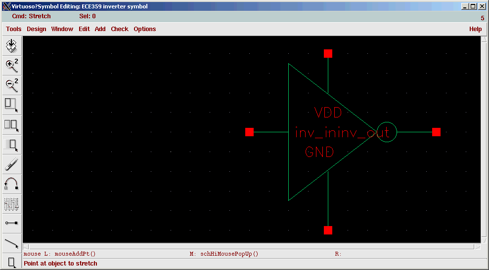
If you don't like this rectangular symbol that is automatically created by the tool, you can create a symbol of you own.
- Editing the shape
of the symbol icon.
You can do the following operations on your symbol:
(1)Deleting/replacing some existing parts(2)Adding new geometric shapes
(3)Changing the locations for pins and instance name
(4)Adding new labels
The figure below is an example for a manually created inverter symbol.
Logic simulation with Verilog-XL
We use Verilog-XL to simulate our designs at logic level. In another word,
we can only check if our design if functionally correct by using Verilog
simulation. We will not be able to know, for example, the transient behavior
of the circuit. Thus we will not be able to know the delay and timing
information for the circuit. To simulate the transient behavior, we should
use Cadence SPECTRE which is very similar to SPICE.
Still, Verilog simulation is very important. A circuit has to be verified
to be functionally correct before we look into its transient behavior.
This section talks about how to write a Verilog "testbench" for the schematic
we created and simulate its behavior. In order to use this tool, only minimal
knowledge of Verilog is required (basically on how to supply the stimuli
during the simulation).
- Start Verilog-XL
In the schematic design window, click on Tools-> Simulation->Verilog-XL to start the verilog-XL. A pop up dialogue box will appear.
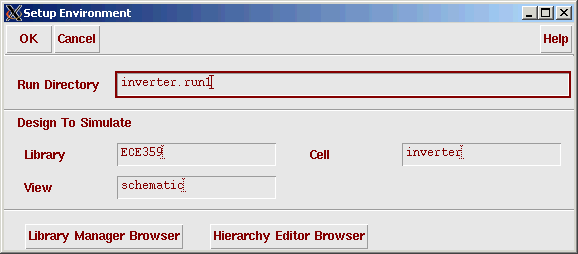
Use the default settings would create a directory named inverter.run1 under the cadence run directory for the verilog simulation. We can specify another path if needed. In this case, we use the default settings. Now a Verilog simulation window appears.
- Create stimulus file
Now in this Verilog simulation window, click on
Stimulus->Verilog..., a pop up message box appears.
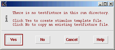
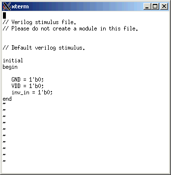
For the first run, since we do not have a stimulus file yet, we click on Yes. A template file named testfixture.verilog has been created for us and a new pop up window appears.
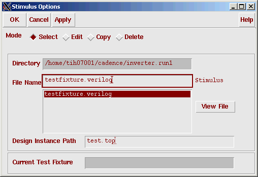
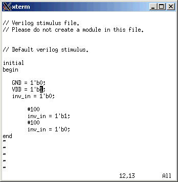
Choose testfixture.verilog as our stimulus file. Now we can modify this file to supply the stimuli during the simulation. Use any text editor to edit this file under the simulation directory (./inverter.run1/testfixture.verilog in this example). The orginal file is shown in the left window below. Now we create a square wave for the input by letting inv_in to be "1" at 100ns and "0" again at 200ns. The modified simulation file is shown in the right window below.
- Simulate
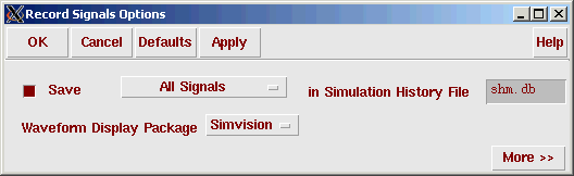
Before we start simulation, we should record all the signals that we want to
display later. Click on Setup->Record Signals
and record All signals in the simulation window
so that we can record all the signals during the simulation to help debug our
designs.
Now click on Simulation->Start Interactive in the simulation window. The simulation initiates. Click on Simulation->Continue to complete simulation. The simulation window looks like below when it completes.
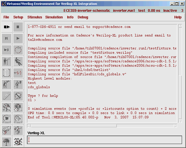
If we run into any problem in the simulation, we can check on the si.log in the simulation directory (~/run/inverter.run1 in this example.)
- View Waveforms
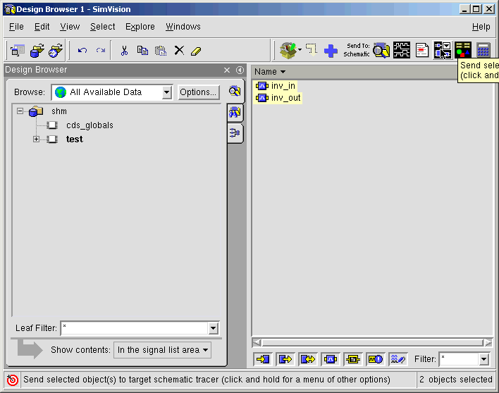
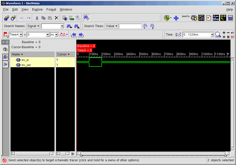
We can use a tool called "Signalscan" to view the results in a waveform format. Click on Debug->Utilities->View Waveform in the simulation window. The waveform window appears.
In the waveform tool window, click on Windows->New->Design Browser, a design browser window pops up. Click on test in the Design Browser window. Select all the signals interested (in this example both inv_in and inv_out) by clicking on them in the right window. Finally Click on "Send selected object(s) to target waveform window" button to display the waveforms in the waveform window.
Circuit simulation with Spectre
Spectre is a
Cadence version of the SPICE circuit simulator. The syntax of Spectre is
compatible with SPICE simulation. By Comparison to Verilog-XL, Spectre lets you
simulate transient behavior of your circuit at the transistor level. In this
section, we are going to simulate the inverter we created to confirm that it
operates as we expect.
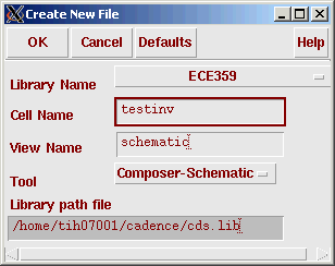
- In CIW window, go to File...->New...->Cellview
A Create New File window appears as below. Fill it out and click OK.
Then a new Virtuoso Schematic Editing window appears.
- Add an instance of the new
inverter symbol that we just created.
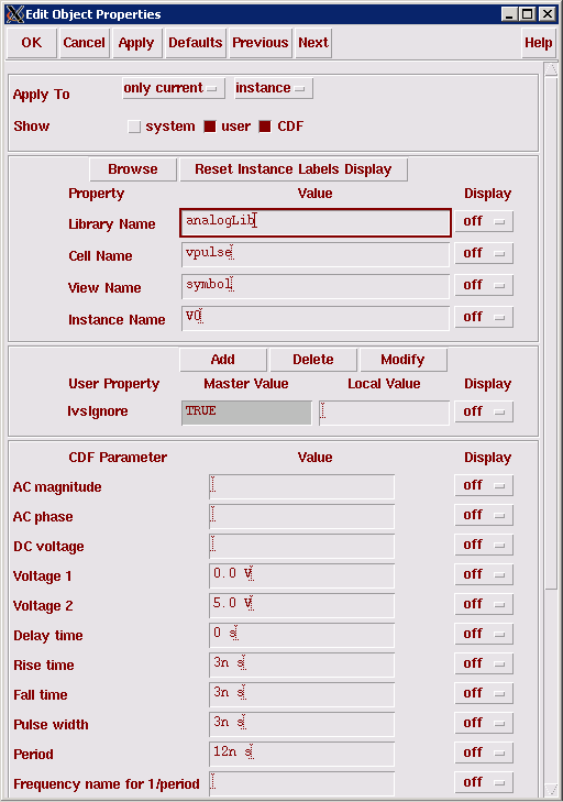
- Add a vpluse
instance from the analogLib library with properties as shown below
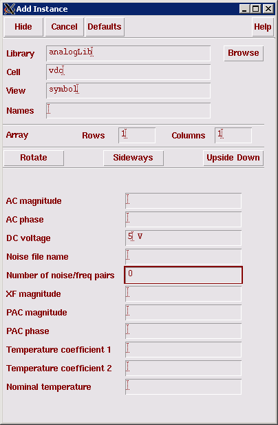
- Add a vcd
instance from the analogLib library with properties as shown below
- In Vistuoso Schematic
Editing window, go to Add...->Wire, connecting all the
components as shown below.
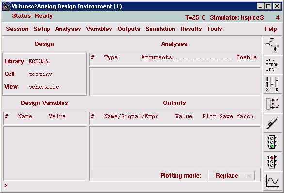
- In the Virtuoso Schematic
Editing window, go to Tools...->Analog Environment, an
Analog Circuit Design Environment window appears as shown below
Go to Setup->Simulator/Directory/Host..., a new window appears as shown below. Choose spectre.
Go to Setup...->Model Libraries..., a Model Library Setup window appears. Click Browse... button and then choose the models directory and then choose the ami05scs model. Click Add as in figure below, and then click OK.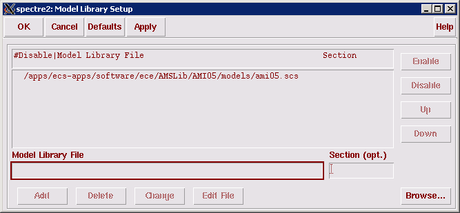
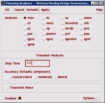
In the Analog Circuit Design Environment window, go to Analysis¡-> Choose¡, and fill out the form according to the figure below.
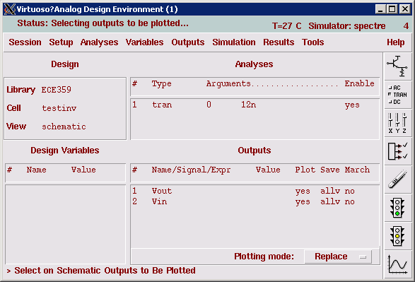
In the Analog Circuit Design Environment window, go to Outputs...->To be Plotted...->Select on Schematic. Than go back to the testinv schematic window and select the Vin and Vout wires. Note, the wires should change color, and the signals should be added in the outputs window as shown below.
-
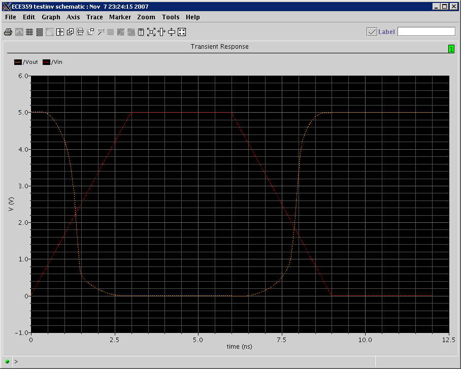
In the Analog Circuit Design Environment window, go to Simulation...->Netinst and Run. The plot of the simulation should appear in a Waveform Window as below.
Custom Layout with Virtuoso
By now, we have already created the schematic and have simulated our design with verilog-XL and spectre. The next step in the design process is to create the layout for the circuit. A layout is basically a drawing of the masks from which your design will be fabricated. Therefore, layout is the most critical step in the design process because it determines whether your design is finally going to be work or not.
Before we get into the layout, first we need to choose the design process we are going to use for the layout. This has in fact been specified when we attach our designs to a specific process when we create the library. In our project, the design process we are going to use is the AMI C5N process, i.e., CMOS 0.5 micron N-well process. It has 3 metal layers and the smallest feature size (generally the gate length) for this process is 0.5 micron.
The design rules we will be using for this process is the MOSIS Scalable CMOS design rules, more specifically, SCN3M_SUBM. This SCMOS design rules specifies the lambda to be 0.3 micron, i.e., the smallest feature size to be 0.6 micron, which is slightly bigger than 0.5 micron. When we use the tool to create the layout, we sometimes see some difference between the design rules from MOSIS and from our tool. If that's the case, please conform to the tool's requirement.
Now we give a tutorial on Virtuoso through creating an example layout for the inverter cell.
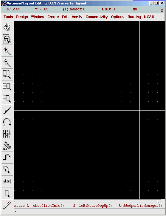
- Create a layout cellview
In the library manager window, click on the File -> New -> CellView. Choose tools as Virtuoso.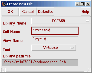

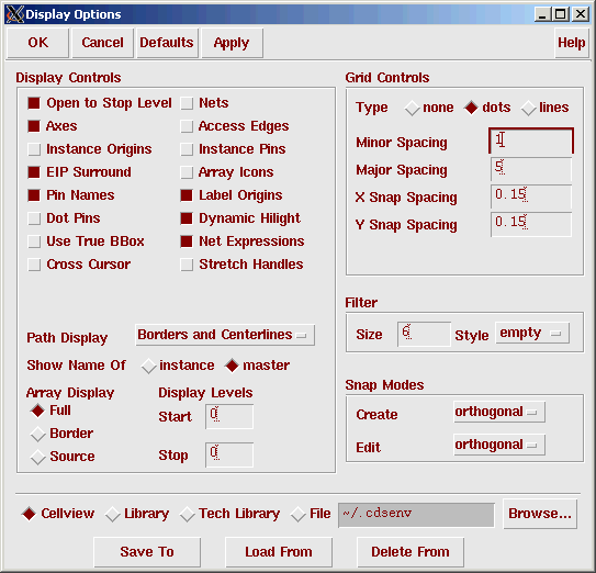
- Change display options
To display the layout properly, we can customize the display options. Click on Options -> Display in the layout window and the following window pops up.
- Draw layout shapes
Before we start to draw the layout, we should understand that each shape in a layout is associated with a layer. Basic layers in AMI C5N process include Nwell; active; N-select; P-select; poly; metal1,2,3; contact; via1,2; glass; pad. We will not use P-well in the AMI C5N process. There are a few layers that are used just to help layout, but does not correspond to any physical layer. For example, text layer is used to annotate the design. Cap_id, res_id and dio_id are used for layout extraction. If we want to draw a shape of a certain layer, we should click on that layer in the LSW before we draw any shape.
There are two basic types of shapes we can draw, path and polygon. Path is often used to represent "wires". Thus we often use paths to draw metal 1,2,3 and poly. This is not a restriction, but rather a common pratice. In fact, you can use path for any layer and you can also use polygon for any layer. To specify a path, click on Create -> Path in the layout window and the following windows appears.
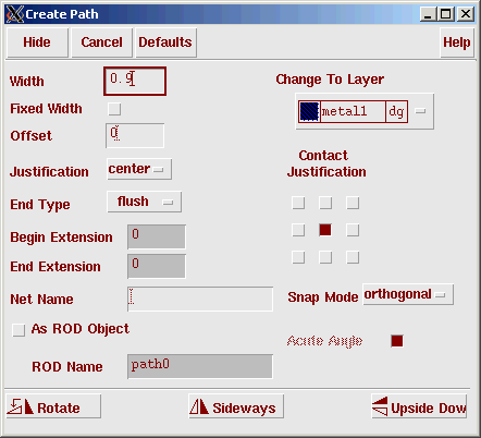
In this window, we can specify the width for the path we draw. The default value in the width is the minimum width of the layer (metal1 in this case). We can also specify the draw style like "justification" and "end type" etc. Now we can activate the layout window and click at the point where you want the wire to start and click at every point where you want to change the direction of the wire till finally you end of the wire by double clicking at the endpoint.
The other type of the shape is polygon. Polygons are generally used to represent the "non-wire" layers that In the layout window, click on Create -> Rectangle. The following window appears.
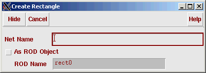
Now in the layout window, click on the two diagonal corners of the rectangle, we can create a rectangle.
We can also click on Create -> Polygon in the layout window to create a polygon. To draw a polygon, we should start by clicking at one of its vertices and then click at the rest of its vertices in order till we finally click at the starting vertex to form a closed shape. The following window shows a metal1 wire created by path, an nwell created by rectangle and an nwell created by polygon.
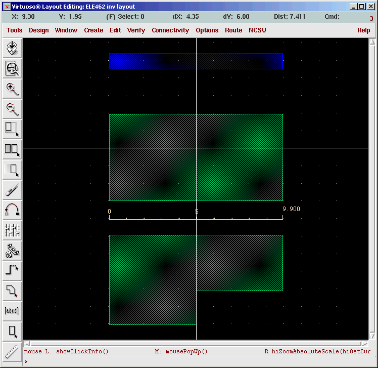
In order to know size of the polygon we just draw, we can use the ruler to measure the length and width of the shape. In the layout window, click on Window -> Create Ruler. Click at the begining and ending endpoints of the line fragments you want to measure and the distance will be shown in the layout window. In the above figure, we know that the widths of the wire and the well are all 9.9 microns. To remove the rulers, click on Window -> Clear all rulers.
A special note to contacts: In general, Contact is of fixed size. In AMI C5N process, contacts are of fixed size 0.6 X 0.6 micron. We can either draw the contacts ourselves or add an instance from the library.
- Create an inverter
The AMI C5N process is an Nwell process, thus the substrate is p-substrate. The P-transistor should be created inside the Nwell and the N-transistor should be created outside the N-well on P-substrate directly. We will create an inverter as shown below with the following steps.
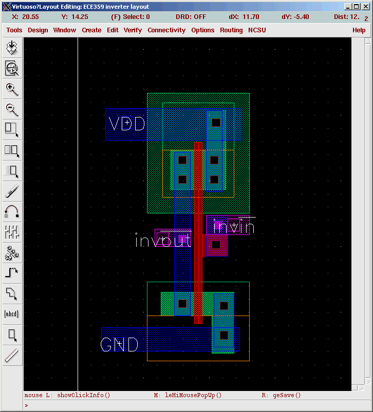
1. Create an N-well. In our case, the N-well is 7.8 X 9.15 micron
2. Create N-select and P-select. Divide the N-well into two regions. One region is P-select, it is used for the P-transistor, the other region is N-select, it is used for the N-well tub-tie. In our case, the two regions abut each other. The size for P-select is 5.4 X 3.6 micron and the size of N-select is 5.4 X 3.3 micron.
3. Create active. Note we use layer active for both P-active and N-active. If the active is within P-select, it is P-active, if it is within N-select, it is N-active. We have created a 4.2 X 3 micron active in the P-select for the P-transistor we are going to create.
4. Create the poly as the gate. In the middle of the P-active, we add the poly wire of 0.6 micron wide (i.e. 2 lambda). This creates the P-transistor.
5. Create contacts and tub tie. The poly has divided the active regions into source and drain. In order to connect the source and drain to metal, we need to create contacts. In our case, we have created two contacts for both source and drain. We have also created a contact as the N-well tub tie to connect the N-well substrate to the power source (in PMOS case, VDD). The tub tie is created in the active region (in this case N-active) to enable Ohmic contact.
6. Similarly, we can create the NMOS transistor following steps in 2-5. The only difference is that there is no well for the NMOS transistors. The NMOS transistors are created directly on top of the P-substrate.
7. Create power and ground wires. The VDD rail is generally above the the cell and the GND rail is generally below the cell. In general, the power and ground rails have a fixed spacing between them so that different cells can easily be connect in a row.
8. Connect the NMOS and PMOS transistor to form an inverter. In the layout window, use metal1 wires to connect the drain of the PMOS and NMOS together and connect the source of PMOS and NMOS to the metal wires for VDD and GND respectively.
9. Create the input and output pins. To be consistent with the schematic we created before, we use inv_in and inv_out for the input and output. In general, we use metal1 to connect intra-cell components and use metal2 and metal3 for inter-cell components. Because of this, we add a via at the output and for the metal2 wires. At the input, since metal2 cannot be connect to the poly directly, we first add a contact between metal1 to poly and then we add a via between metal2 to metal1 on top of the contact. (NOTE: AMI C5N process allow stacked contacts).
To define a pin, first click on Create->Label. The following create labels window appears.
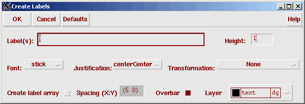
In this window, fill in Labels with inv_out. Then, click on Create->Pins From Labels. The follwing window appears.
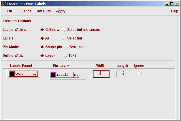
Click OK to convert the label you have just created into pin.
¡¡
- Check and save your design
Before saving the design, we hope to make sure that the design has comform to the design rules. As careful as one might be, it is very hard for a designer to avoid all the design rule errors. To perform the design rule checking, click on Verify -> DRC... in the layout window. A pop up dialogue box will appear.
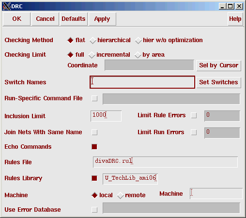
For a small circuit like an inverter, it is OK just to run the DRC in the flat mode since the running time is short. For a big layout, however, it is wise to run the DRC in a hierarchical mode. In general, hierarchical mode is faster than flat mode, especially for a large layout composed of iterative structures. However, hierarchical DRC might not be accurate in some rare cases. Thus it is a good practice to check a big circuit with hierarchical DRC first and then run a flat DRC by the end. Click on the OK button and the Diva DRC tools will be invoked the check the design and reports the errors in the CIW.
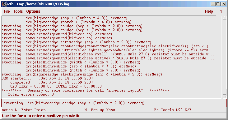
In this case, the CIW above shows that there is no error found in the DRC process. If, however, there is any error reported, the layout will be marked and CIW will indicate what kind of violations there are. You can then modify the layout and run the DRC again till there is no DRC errors.
After the cell has been checked, click on Design -> Save... in the layout window to save your design.
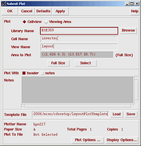
- Plot your design
In the layout window, click on Design->Plot->Submit and the following window pops up.
Click on plot Options... and another window appears.
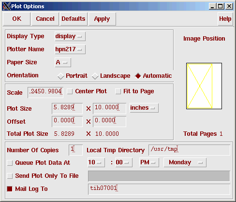
Modify the Plotter Name to be EPS and Paper Size to be 8X10.5 inches and select Send Plot Only To File inv.ps. Click on OK and the layout postscript file will be created under your cadence run directory.
- Hot keys
i: Add instances
q: Edit properties
r: Add rectangles
p: Add path
P: Add Polygon
ctrl+p: Add a pin
l: Label a wire
z: Zoom in
Z: Zoom out by 2X
ctrl+z: Zoom in by 2X
f: fit the layout in your layout window
right mouse button: repeat last command
In order to show the pin names, select Pin Names in Display Controls. You can also change the Grid Controls to alter the Minor Spacing and Major Spacing. But do not change the X Snap Spacing or Y Snap Spacing and leave them to be half lambda. Finally you can save your changes to the .cdsenv file.
¡¡
Layout extraction and Layout Versus Schematic (LVS) with Diva
We have created the layout as well as the schematic for an inverter, but how do we know they represent the same circuit? One way to verify this is by generating a circuit netlist from the layout and comparing it with the netlist for the schematic. This is the essence of the the LVS tool. Thus in order to use the LVS tool, we have to first extract the layout to the netlist.
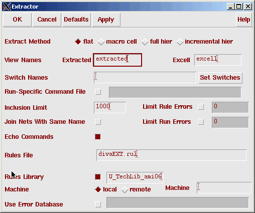
- Layout extraction
In the layout window, click on Verify -> Extract... . The following dialogue box pops up.
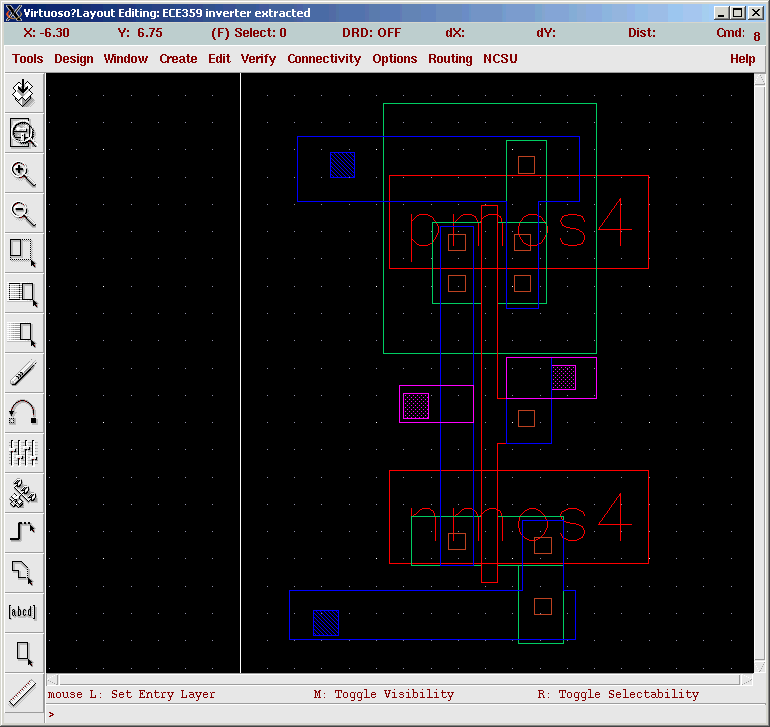
Check the CIW window to make sure the layout extraction process runs through sucessfully. After the process is done, check the cell in the library manager and you will see an extracted view. Open the extracted view and the following layout window appears.
- Layout Versus Schematic
From the extracted window, choose Verify -> LVS... . The following dialogue box appears.
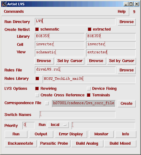
Specify the Run Directory as well as the cell and views you want to compare. If you are running LVS on a huge layout, it is better to create a run directory under /tmp so that the LVS won't run out of disk space. If you already have executed an LVS under the specified directory before, a window will pop-up which might say The selected LVS rule directory does not match the run form . Just click on Form contents and OK.
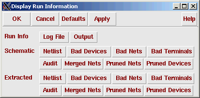
Click on the Run button. The tools will prompt you if the LVS is sucessfully or not. To see if the job is still running, you can click on the Job Monitor... button in the LVS window and a pop up menu will appear to tell you the status of the current process. If the process is not successful, you can click on Info in the LVS window. The following window appears. You can check the log file to figure out the run time problem for LVS.
If the LVS runs through successfully, click on Output in the LVS window and the result is displayed.
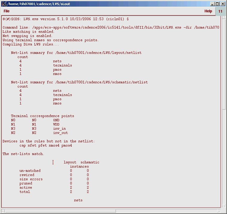
In our case, the LVS reports that there is no difference between the extracted circuit and the schematic. If, however, there is some difference, Click on the Error Display button in the LVS window and following window appears.
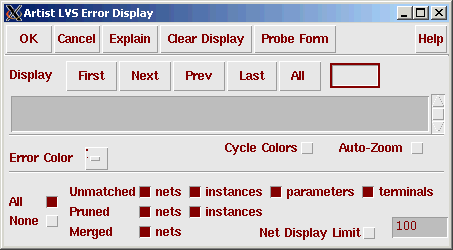
Click on First and other buttons to display the current or all the errors in the extracted layout window. The errors are highlighted by a green dot. To get more information about the error, click on the Explain button. Modify the layout or schematic appropriately and rerun the LVS till your design is perfectly matched.
Post Layout Simulation
We have used spectre to simulate the schematic before, but the layout is different from schematic in the sense that some parasitic capacitance and resistance information cannot be obtained in the schematic. For example, the schmatic editor cannot determine the wire capacitance and resistance information because schematic only worries about netlist and they do not have the wiring information (i.e. how the wire is routed). Because of this, it is very important to perform a post-layout simulation from the extracted view since it is closer to the reality.
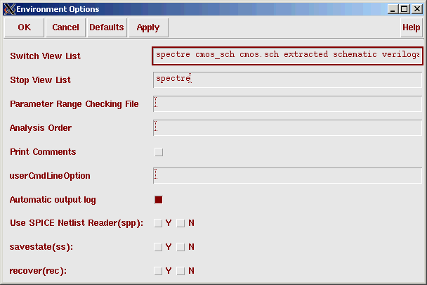
Follow the steps in circuit simulation with Spectre to simulate the circuit. Before running the simulation, go to Setup->Environment... in Virtuoso Analog Design Enviroment window, and add 'extracted' in front of 'schemetic' in Switch View List Box.
After running the simulation, we will get the simulation result as the figure below.
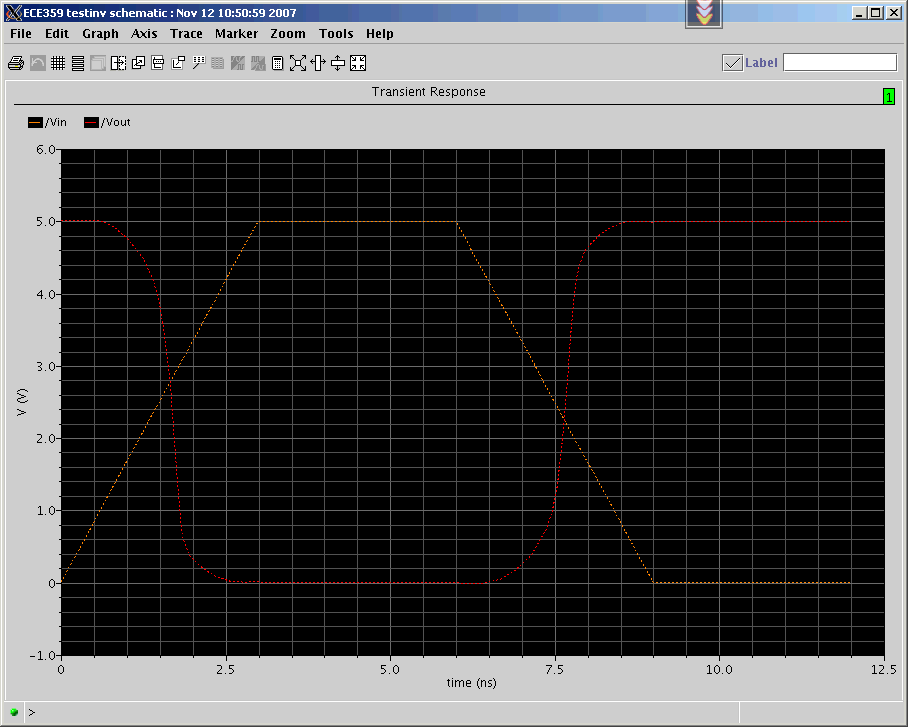
This simulation should be used to determine the final circuit behavior. If the timing of the circuit doesnot satisfy the timing requirement. We will have to modify the layout or even the schematic to adjust the size of the transistor and wire or even reconstruct the logic until the constraint is finally satisfied.