Engineered Nanostructures for Authentication
Engineered Nanostructures for Authentication
The increasing proliferation of counterfeit electronic components threatens both commercial and military systems in the areas of product performance, reliability and dependability. They are of great concern because of (i) the negative impact that they can have on innovation, (ii) the threat they pose to the welfare of consumers, and (iii) the substantial resources that might be channeled to criminal and other networks.
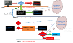
The development and demonstration of different counterfeit detection technologies extending from optical inspection to rather sophisticated x-ray imaging have been able to identify certain sets of counterfeit defects. These techniques are yet to be consolidated such that counterfeit identifications are conclusive and without any false positives. Different counterfeit identification schemes such as DNA, Nanotag, RFID, PUF provides solutions but do not offer a comprehensive solution. Counterfeit detection still has much intrinsic subjectivity, and thus the confidence level of the associated results is lacking. Technologies such as DNA and RFID though provides excellent authentication accuracy are slow in authentication of counterfeit electronic components as well as are prone to imitation. Nanotags do not suffer from the same limitations but slows down the process time and are expensive. The challenge is to be able to incorporate counterfeit identification signatures in COTS electronic components alleviating the requirement of a suite of expensive and time consuming counterfeit detection schemes.
The Engineered Nanostructures (ENS) utilizing some unique optical properties of tailored nano-structures does not suffer from the detrimental attributes of any one of these technologies and offers an inexpensive but reliable technology to ensure authenticity of electronic components.
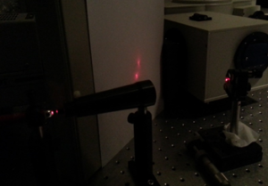
Engineered submicron features modifying some of the physical properties of the IC capping material are being proposed as a tool for the identification of counterfeit ICs. The submicron signature invisible to the naked eye but visible under high magnification optical microscopes (>x1000) modify the optical properties of the capping material and detected by using inexpensive and fast optical probing such as shining a laser pointer on the surface of the IInitial proof of concept validation successfully demonstrated the effectiveness of the proposed counterfeit inhibition technology. The figure shows a simple demonstration using laser pointer to excite the engineered nano-signature (ENS). The presence of ENS generates the two distinct reflections, one from the surface of the IC capping layer and an additional reflection (lower spot) due to ENS.
It is believed that the proposed technology offers the following:
- A tool allowing identification of good ICs, already been capped and in post design phase.
- Impossible to resurface and re-introduced in the market as any retooling of the surface destroys ENS.
- The ENS array can be tailored to provide unique signatures unique to the IC. This random signature either unique to a family if ICs or an individual IC may be entered into an IC identifier register for future reference and cross-verification. This will allow the detection of over-produced or counterfeit ICs as the counterfeiters will not be able to re-generate the random ENS unique to an individual IC even if they are able to imprint one particular ENS.
Publications:
- Fabrication of robust nano-signatures for identification of authentic electronic components and counterfeit avoidance, K Ahi, A Rivera, A Mazadi, M Anwar, International Journal of High Speed Electronics and Systems 26 (03), 1740006, 2017
- Encrypted electron beam lithography nano-signatures for authentication, K Ahi, A Rivera, M Anwar, International Journal of High Speed Electronics and Systems 26 (03), 1740017, 2017