UConn ECE Professors On The Cutting Edge of Nanotechnology Research
By: Eli Freund, Editorial Communications Manager, UConn School of Engineering
Since the invention of the transistor in the mid 20th century, engineers have been expanding on the field of nanotechnology, which is the study and development of materials, processes, and devices that are on the atomic, molecular, and supramolecular level. From fabrics that repel liquids to a 10mm processor from Intel, the possibilities are endless—and a few faculty from the University of Connecticut Department of Electrical and Computer Engineering are working hard to advance the field to new levels.
One of those faculty members, Associate Professor John Ayers, who has been at UConn for 30 years, started out in industry, where he developed his passion for the field.

“I first developed a passion for nanotechnology while working in the integrated circuit fabrication facilities of Fairchild and National Semiconductor in the 1980s, and this passion expanded when I began research on epitaxial structures at Rensselaer Polytechnic Institute and Philips Laboratories.”
Epitaxy is a process used most commonly, on the commercial side, in the semiconductor industry where crystal layers are stacked on top of each other to form a film.
Ayers said that once he left industry and joined UConn, he was able to create new processes and help companies in research and development.
“After arriving at the University of Connecticut in 1990 I established research in the area of nanoscale epitaxial structures and published two editions of the top book in this field. We invented a nanoscale defect-engineering approach, called patterned heteroepitaxial processing (PHeP) or dislocation sidewall gettering (DSG) which has been commercialized in LED flat-panel displays as well as nearly every infrared focal plan array manufactured today. More recently we have collaborated with Silicon Valley researchers to develop the processing and materials for high-performance SiGe digital integrated circuits. We continue to focus on the engineering of epitaxial nanostructures, with applications in high-efficiency, multi-junction solar cells, efficient solid-state lighting, and high-speed transistors for smart phones and autonomous vehicle radars.”
Another faculty member focusing research on nanotechnology is Associate Professor Helena Silva, who found her passion for the field during her undergraduate years.
 “During my undergraduate studies in Portugal, I had the opportunity to work in a research lab on electronic devices, specifically amorphous silicon thin film transistors which are used for large-area electronics (displays, medical imaging sensors, solar cells). Since then I have developed an interest in all types of electronic materials, device fabrication, and characterization techniques.”
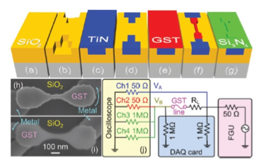
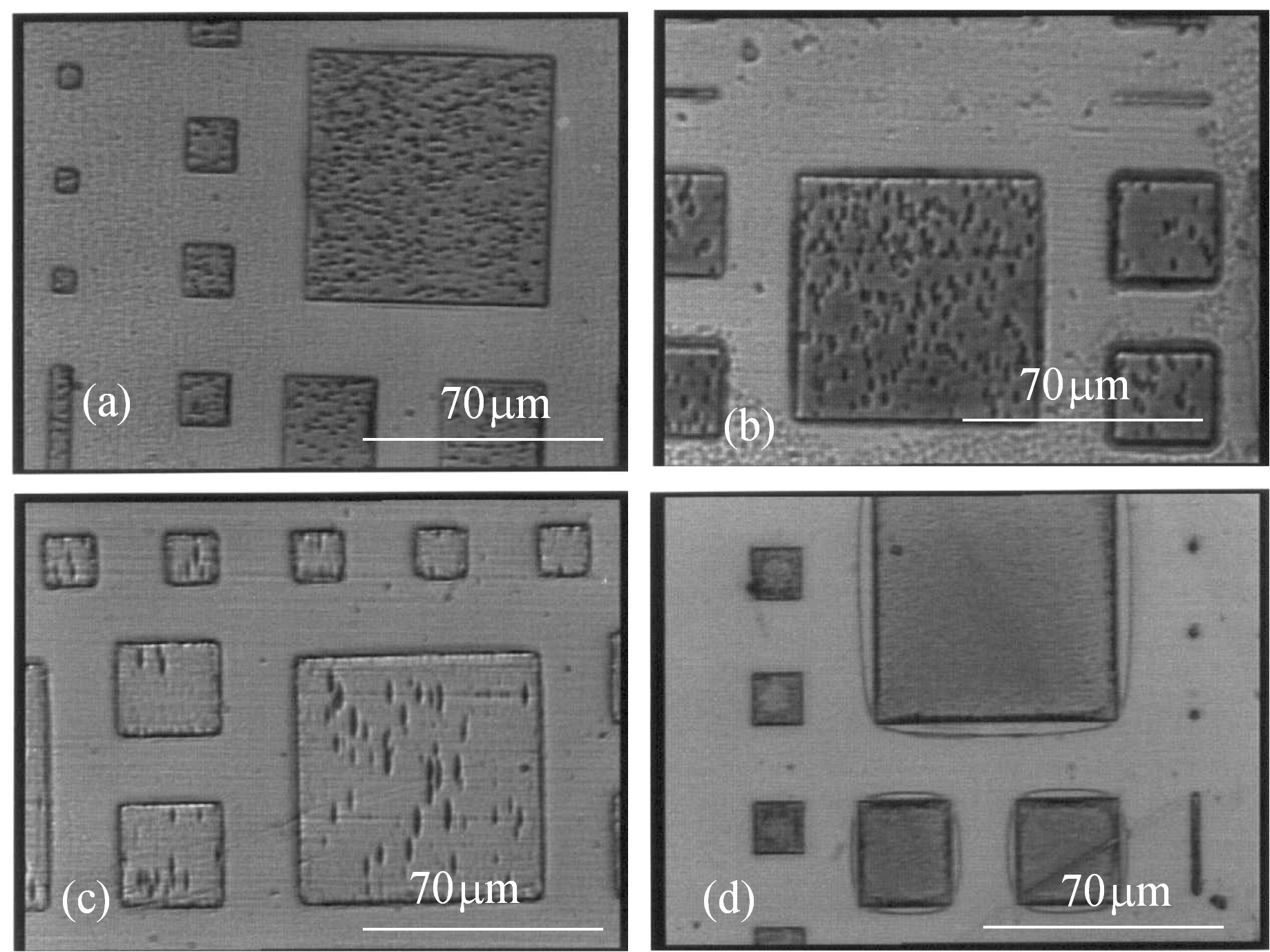
Silva, who has been at UConn since 2006, currently works on phase-change electronic memory devices. This is a new non-volatile memory technology with the potential to replace flash memory for significantly faster Solid-State Disks (SSD) type storage.
While both faculty members feel like the field is still developing, Ayers and Silva both agree that there are boundless possibilities.
“The future of nanotechnology and nanoelectronics involves presently unimaginable advances in displays, digital communications, computing, transportation, and energy. The complexity of the materials, devices, and processes will require a shift from empirical, cut-and-try approaches to one involving sophisticated models and virtual design,” Ayers said.
|
F. Dirisaglik, et al., “High speed, high temperature electrical characterization of phase change materials: metastable phases, crystallization dynamics, and resistance drift,” Nanoscale, 2015,7, 16625-16630 (2015).
|
X. G. Zhang, et al., J. Appl. Phys., 91, 3912 (2002).
|